

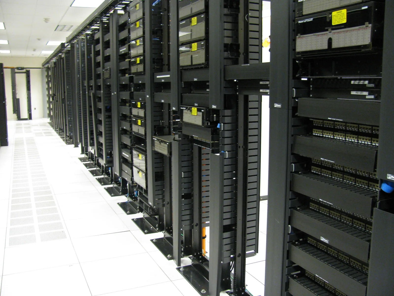
Compute capacity is often the first metric discussed for AI infrastructure. But in a coordinated computing system, useful computation also depends on data reaching the right place at the right time.
If communication cannot keep up, adding compute resources may not deliver a corresponding increase in useful output. Optical interconnects must do more than make one link faster: they must keep more data moving reliably within power, distance, space and cost constraints.
Changes in technology architectures respond to these constraints.
Users Need More Than a Higher Headline Data Rate
For system architects, bandwidth matters—and so does the cost of supporting it.
An interconnect must address reach, energy per bit, interface and component footprint, and serviceability after failure. There is no universally optimal answer independent of the application.
Rack-to-rack links, connections near switch ASICs and compute-chip interconnects have different reach, topology and serviceability requirements. The advantages of one packaging approach cannot be generalized unconditionally to every location.
When examining a roadmap, first identify the interconnect segment it addresses, then evaluate its value.
Why Optics Is Moving Closer to the Chip
Moving electro-optical conversion closer to chips is one approach some architectures use to shorten high-speed electrical paths and improve bandwidth density and energy efficiency.
The Skin Effect: A Physical Constraint on Copper Channels
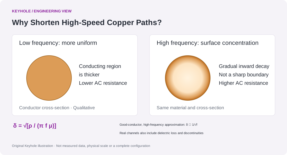
Copper conducts electricity, but high-frequency current is not distributed nearly uniformly across its cross-section as in an ideal DC case. Alternating current produces a time-varying magnetic field, and induction affects internal electric fields and current distribution. At high frequencies, current density concentrates near the surface and decays inward: theskin effect. This does not mean current exists only at the surface or disappears entirely inside the conductor.ADI technical explanation
For a uniform good conductor under the usual high-frequency approximation, skin depth is:
δ = √[ρ / (π f μ)]
Here, ρ is resistivity, f the sinusoidal component frequency and μ permeability. δ is the depth at which current-density amplitude falls to approximately 1/e of its surface value, not a sharp boundary. With unchanged material parameters, quadrupling frequency halves skin depth.
A thinner effective conducting region increases AC resistance per unit length. Under sufficiently developed skin effect and applicable geometry/material assumptions, the skin-effect resistance term grows with the square root of frequency. Real copper channels also have dielectric loss and connector/via impedance discontinuities; not all channel loss is caused by skin effect.Keysight transmission-line modeling reference
Digital signals contain multiple frequency components. Frequency-dependent attenuation and phase response alter the received waveform and complicate recovery. Data rate is not itself a single sinusoidal frequency; requirements also depend on modulation, edge characteristics and channel design.
Shorter high-speed electrical paths therefore have a physical rationale: less lossy copper traversal leaves more link margin. This does not make copper obsolete or optics lossless. Moving conversion closer still requires a comparison of distance, efficiency, cost, optical coupling, packaging and maintenance.
The argument is not simply that light is more advanced than electricity. Electrical transmission and signal recovery have costs. NVIDIA relates shorter paths, signal-integrity design and reduced need for certain external DSPs in its CPO architecture. That architecture-specific choice does not mean all optical interconnects eliminate DSPs.Architecture reference
NVIDIA's 2025 CPO discussion covers co-design of photonic and electronic chips, fiber connections, lasers and packaging. Intel's 2024 OCI chiplet demonstration was co-packaged with a CPU and carried live data. Both illustrate optical integration at different system locations, not identical applications or maturity levels.NVIDIA technical reference、Intel demonstration reference
From an engineering perspective, the evolution redistributes problems rather than eliminating them. Electrical paths can shorten, while optical access, thermal conditions, manufacturing and serviceability must be reorganized.
Users must compare whole-link benefits and costs, not isolated device power. Sources, thermal control, connections and field maintenance remain part of system assessment even when a local electrical path improves.
Closer to the chip is a system-level trade-off, not an unconditional improvement.
What Concerns Users as Integration Increases?
Device and optical-engine teams need to know whether a design remains achievable under actual manufacturing and assembly conditions. Good performance under ideal conditions does not guarantee consistency across channels, samples or repeated assembly.
Packaging teams face more specific questions: Did the change originate inside the chip or at a coupling/connection interface? How large is the before/after difference? Is the change repeatable after reconnection?
For quality teams, one reading is a starting point. They also need the actual path, reference conditions and process stage. Data saved at every station may still be incomparable without this context.
These challenges explain why testing should be planned with design, packaging and manufacturing, rather than treated only as a final release operation.
From One Number to Complementary Measurement Evidence
Transmission, reflection and channel differences answer distinct questions.
Transmission assesses optical power changes through a device or link; reflection reveals discontinuities and returning light that may affect a system. Appropriate methods and configurations can add spatial clues. Channel comparison distinguishes individual-path behavior from the overall distribution.
These measurements complement but do not replace one another. Acceptable optical loss does not guarantee high-speed signal quality or BER, and spatial localization cannot identify every failure mechanism. High-speed modulation and communication performance require suitable oscilloscopes, BER test equipment and system validation.
From Prototype to Application: What Still Needs Verification?
A link operating in the laboratory demonstrates that one set of devices and conditions works. Manufacturing and assembly require further checks: channel loss distributions against budgets, stability after repeated assembly, and temperature effects. Preserve paths, references and sample records—not only a pass result.
Shorter copper paths provide electrical margin, while closer optical conversion adds optical access, packaging and thermal requirements. Compare both within the same link: do electrical improvements survive optical loss, assembly variation and system validation? This is closer to users' real decisions than an isolated component parameter.
Further Reading
- CPO, Optical Engine and Multichannel Interconnect Solution
- Next in this series:As Optics Moves Closer to the Chip, Why Must Testing Move Upstream?
Editorial note: This engineering analysis draws on public technical material. It does not guarantee production scale, replacement timelines or performance benefits for a particular architecture. Third-party examples do not indicate customer relationships or validation of Keyhole products.