

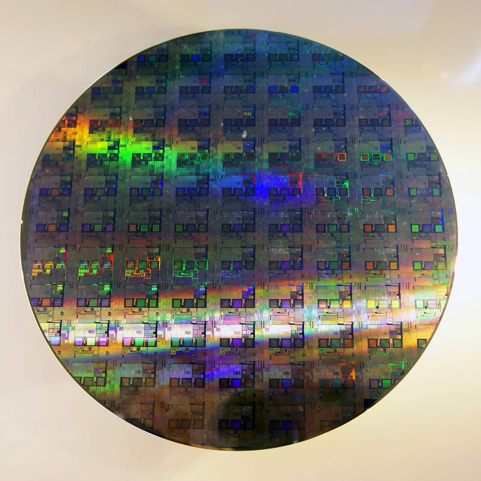
An anomaly detected at final test has been found—but is not necessarily easy to resolve.
After coupling, bonding and packaging, engineers must ask more than whether a device passes: Where did the anomaly originate? Can prior processing be recovered? Which step should change for the next batch?
Closer integration of photonic/electronic chips, fiber interfaces and advanced packaging makes early evidence valuable. Testing upstream is about making better-informed decisions earlier, not simply measuring sooner.
Why Final Test Alone Is Not Enough
Final-product results combine effects from chip structure, coupling, interfaces, packaging stress and measurement conditions.
Without earlier records, a final anomalous trace cannot readily distinguish a pre-existing device issue from an assembly-induced change. It may support acceptance or rejection without guiding process improvement.
FormFactor's silicon photonics wafer-testing material emphasizes testing functional chips before stacking and packaging for heterogeneous integration. This illustrates the role of upstream screening.Public reference
Earlier reliable detection of existing anomalies may avoid further processing of unsuitable devices. Actual savings depend on defect distributions, test cost, screening accuracy and subsequent processes—not simply on moving a test earlier.
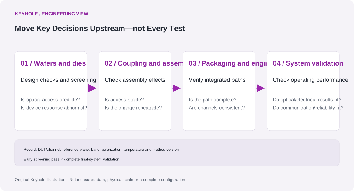
Move Key Decisions Upstream, Not Every Test
Replicating every final-test item at wafer level may be infeasible or uneconomic. Optical access, device states and measurement objectives differ by stage.
Begin by defining the decision each stage must support.
| Stage | Decision to Address | Value for Subsequent Work |
|---|---|---|
| Wafers and bare dies | Under applicable conditions, does response match design expectations? Are there anomalous distributions worth investigating? | Support screening, design verification and process observation |
| Coupling and assembly | Is optical access stable? Which parameters change after assembly? | Narrow coupling and assembly investigations |
| Packaged devices and optical engines | Is the actual optical path complete? Are channels consistent? | Verify post-integration optical behavior |
| System validation | Do optical, electrical and high-speed communication performance jointly meet operating requirements? | Support system-level decisions and confirmation of application scope |
This is a task breakdown, not a universal process standard. The DUT, process and quality requirements determine sequence, coverage and thresholds.
Why Wafer Testing Is Itself Challenging
Moving a measurement earlier does not necessarily make data easier to obtain.
Photonic chips require suitable optical access. FormFactor's edge-coupling material discusses alignment, calibration and automation challenges at wafer level. Access must match device structures and the test system.Edge-coupling test reference
Upstream testing must address both what to measure and whether it can be measured stably and credibly at that stage.
If reconnection variation masks device differences, more early testing can increase misclassification. Excessive alignment or test time for one screen may also require a revised coverage strategy.
Early Screening Does Not Guarantee Final Compliance
Pre-packaging screening reduces some risks but cannot eliminate later defects or cover every operating condition.
Distinguish passing under the present method and threshold from complete final-system validation. The former does not automatically establish the latter.
Wafer transmission/reflection tests cannot replace packaging reliability, full electro-optical function, high-speed signal quality or communication validation. Earlier tests should build layered evidence, not weaken later verification.
Make Data Comparable Across Stations
Before comparing pre- and post-packaging results, establish whether they are genuinely comparable.
Associate device/channel identifiers, bands, optical paths, reference planes, polarization, temperature and analysis versions. When access methods differ, record which effects are referenced or compensated and which remain in the results.
Without context, two values with identical units may describe different measurands.
Upstream testing also requires data to travel with the device. Stations must exchange enough conditions and records to interpret results, not just hand over samples.
The Goal Is Better Engineering Decisions
When defining a workflow, ask which finding at which stage can change the next decision, what access and cost it requires, and what follows from missed defects or false decisions.
Clarifying these questions before selecting instruments, automation and data systems is usually more effective than adding test items first.
Keyhole focuses on giving design, process and quality teams credible evidence at the right stage—not moving every test to the beginning.
Further Reading
- Silicon Photonic Wafer and Chip Test Solution
- Next in this series:Poor Wafer-Test Results: Is It the Chip or the Coupling?
Editorial note: The stages form an engineering discussion framework, not a universal production process or a complete Keyhole production line. Access, coverage, automation and assessment capabilities require project-specific validation.