

MEASURE
Super-resolution optical frequency-domain interferometry
Resolve reflection, loss, defects and polarization-related information along optical paths to establish trustworthy measurement data.
KEYHOLE PHOTONICS · SILICON PHOTONICS TEST
We use super-resolution optical frequency-domain interferometry to investigate light propagation in communication links, and digital twins to relate structure to performance. Our goal is to provide traceable measurement evidence for R&D, process optimization and production quality assessment in high-speed optical communications, silicon photonics and photonic quantum computing.
OUR MISSION
Keyhole Photonics focuses on silicon photonic chip testing across optical communications, silicon photonics, and photonic computing and quantum photonics.
Our approach combines super-resolution optical frequency-domain interferometry with optical digital twins to measure reflection and loss along optical paths, locate anomalies, and relate device structure to performance—helping engineers determine where a problem occurs and which process steps warrant investigation.
Meet Keyhole Photonics ↗FLAGSHIP PLATFORM

An optical vector analyzer platform for silicon photonic chips and optical components, bringing high-resolution reflection, loss analysis and fault localization to R&D, process development and production.
* Some extension capabilities are still under development or validation. Availability, licensing and delivery schedules are subject to the agreed software version and technical documentation.
Explore the Product Platform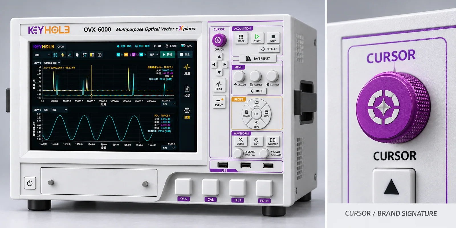
TECHNOLOGY ROADMAP
Analyze optical paths with super-resolution optical frequency-domain interferometry and relate structure to performance through optical digital twins—progressively connecting measurement, diagnostics, traceability and automated testing.
Resolve reflection, loss, defects and polarization-related information along optical paths to establish trustworthy measurement data.
Connect waveguide, coupling and packaging information with device performance to narrow the fault-localization process.
Build traceable test datasets to support process-window analysis and quality assessment.
Planned integration with automation, MES and yield analysis to connect R&D and production data.
THREE APPLICATION AREAS
Our roadmap builds on optical communications, advances silicon photonics, and explores measurement limits in photonic computing and quantum photonics.
Supporting yield improvement in high-speed photonic chips
Mature · Stable · Production-focused02A measurement benchmark for silicon photonic integration
Precision · Integration · Local supply-chain capability03Measurement infrastructure for emerging photonic chips
Emerging · Advanced · Future-facingINSIGHTS
From low-loss fiber to chip-to-chip optical interconnects, follow how optical testing challenges evolve.
Charles Kao and George Hockham propose a theoretical path toward fiber-optic communications.
Historical source ↗Corning develops low-loss optical fiber, helping make fiber-optic communications practical.
Historical source ↗AlphaGo defeats Lee Sedol 4–1, marking a milestone in AI capabilities.
Historical source ↗On November 30, ChatGPT launches as a research preview, giving the public direct access to generative AI.
Launch announcement ↗Silicon photonics and CPO/NPO bring denser optical paths—and demand more detailed measurements.
Keyhole's testing perspectiveNVIDIA Next-Generation CPO Platform ↗Spectrum-X Ethernet Photonics · 2026.01.05The device and wavelength stay the same, yet reconnecting the fiber produces a different transmission result. Understanding polarization helps distinguish device response from input conditions and coupling changes.
Read Insight ↗ Interconnects and ManufacturingMoving from a single path to FAUs, MPOs and multichannel optical engines requires more than fast acquisition. Mapping, switching stability, reference management and anomaly retesting determine whether the results are usable.
Read Insight ↗ Software and WorkflowsA successful remote connection only establishes a control path. A repeatable workflow also needs state synchronization, condition records, exception recovery and version management.
Read Insight ↗ Emerging Applications and R&DProgrammable optical circuits depend on interference, phase and path control. Without understanding loss, drift and input conditions, changes in outputs or counts cannot readily be attributed to computation or quantum processes.
Read Insight ↗ Industry TrendsGrowing compute demand requires faster links and stable connections across more channels under power, space and manufacturing-cost constraints. These constraints explain why optical architectures and test requirements evolve together.
Read Insight ↗ Manufacturing and TestAs chips, optical coupling and packaging become more integrated, discovering a problem only at final test can lengthen the investigation. Moving testing upstream means obtaining useful evidence at the right stage—not simply testing earlier.
Read Insight ↗ Test MethodsLow power, drifting traces or inconsistent repeat measurements do not necessarily originate in the chip. Verify measurement-path stability and reference conditions before separating coupling changes from device differences.
Read Insight ↗ Optical Path DiagnosticsAn end-to-end reading assesses overall transmission but does not directly locate an anomaly. Combining transmission results, spatial information and controlled retesting helps narrow the investigation to a structure or interface.
Read Insight ↗OUR VISION
Focused on instrumentation and sustained development, we aim to extend the precision and practical value of photonic chip testing across optical communications, silicon photonics, photonic computing and quantum photonics.
Help Shape the Next Standard